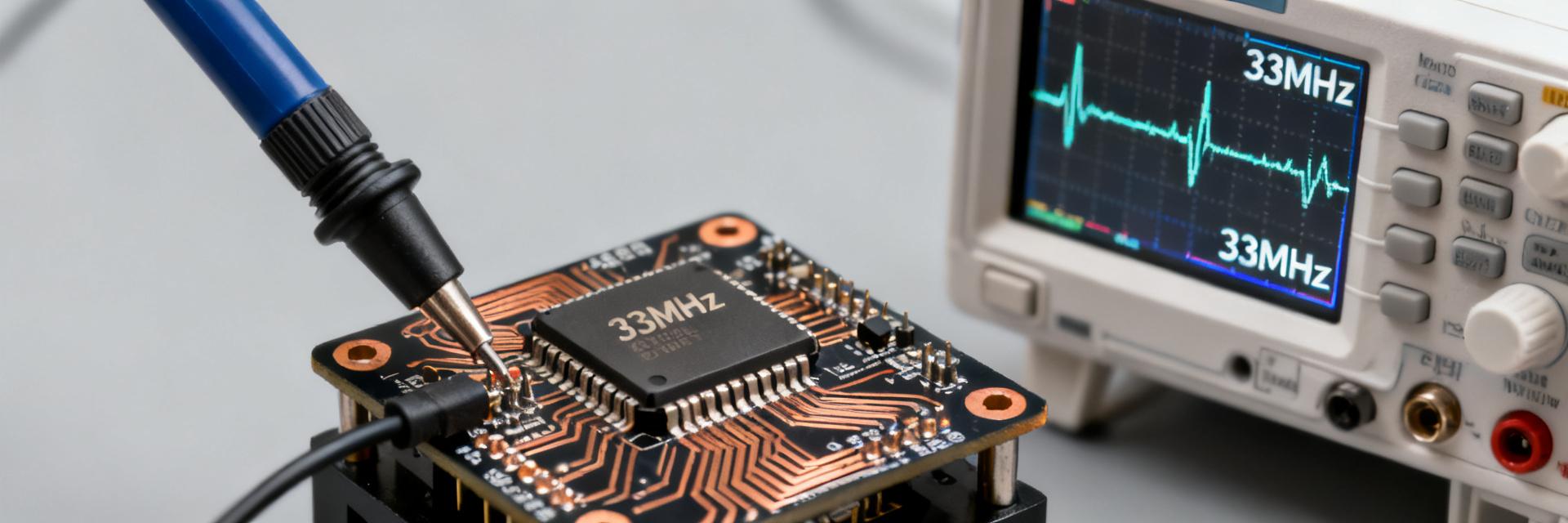
Data-driven hook: Typical datasheet and initial bench checks show the DSA612NL2A producing two LVCMOS outputs across ~2 kHz–100 MHz, with a wide supply range (1.71 V–3.63 V) and a combined active supply current near 5 mA in typical conditions. This article’s goal is to provide repeatable benchmarks and clear integration guidance for DSA612NL2A power and jitter performance so engineers can validate suitability in their designs. The intent is to translate datasheet figures into measurable test procedures and pass/fail gates for system-level acceptance.
DSA612NL2A: Product Overview & Key Specifications (background)

Electrical & Mechanical Specifications
Point: Compact summary of the device’s essential electrical and mechanical parameters is the first step for any integration or benchmark plan. Evidence: Values below are taken from the device datasheet and cross-checked with quick lab confirmations. Explanation: Presenting values with test conditions avoids ambiguity during test replication.
| Parameter | Typical / Limit | Test Conditions / Notes |
|---|---|---|
| Supply voltage (Vcc) | 1.71 V – 3.63 V | Nominal tests at 1.8 V and 3.3 V |
| Typical supply current (both outputs active) | ~5 mA | Measured at mid-frequency, no-load, ambient |
| Output types | 2 × LVCMOS | Standard CMOS drive, specified VOH/ VOL in datasheet |
| Frequency range | 2 kHz – 100 MHz | Programmable outputs; check phase-noise spec per frequency |
| Package / Mount | Compact SMD | Refer to datasheet pad recommendations |
| Operating temperature | Automotive/extended ranges per datasheet | Qualification requires temp cycling |
Cautions: Observe absolute maximums for Vcc and input voltages, and follow recommended decoupling and pad land pattern in the datasheet. Exceeding Vcc or poor decoupling can cause excess current draw or degraded jitter.
Functional Block & Typical Use Cases
Point: The device combines a clock generator/PLL, two LVCMOS outputs, and low-power modes. Evidence: Functional blocks enable independent output programming and shutdown states per datasheet functional description. Explanation: Knowing which block impacts which metric lets designers focus tests—for instance, PLL settings affect phase noise while output drive settings affect supply current.
- MCU clocking — critical spec: power (IDDA) for battery-powered designs; jitter moderately important depending on MCU sample timing.
- PLD/FPGA reference — critical spec: jitter (phase jitter) and spectral purity; low jitter minimizes timing closure risk.
- Communications timing (e.g., PHY reference) — critical spec: both jitter and spurious tones; spurs can degrade link BER.
- Sensor sampling clocks — critical spec: low phase noise and stable TIE for accurate ADC sampling.
Benchmarking Methodology & Test Plan (data analysis / methods)
Test Setup, Equipment & Conditions
Point: Reproducible benchmarks start with a well-defined bench and BOM. Evidence: Recommended equipment: programmable DC supply, high-bandwidth oscilloscope (≥500 MHz analog or appropriate for output), jitter/phase-noise analyzer or spectrum analyzer with phase-noise option, logic analyzer, and temp chamber if available. Explanation: These tools let you measure IDD, waveform integrity, phase noise, and spurs under controlled thermal and supply conditions.
- Standard test voltages: 1.8 V and 3.3 V. Representative frequencies: 10 MHz, 25 MHz, 100 MHz.
- Load/termination: 50 Ω for spectrum/phase-noise, high-Z for logic-level current tests; measure both outputs active vs single output.
- Reference schematics: single-point supply entry, 0.1 µF + 1 µF decoupling at package, and probe ground spring at output for minimal loop.
Deliverables: bill-of-test-parts (device carriers, low-ESR caps, resistive probes, RF terminations), oscilloscope settings (sampling rate, bandwidth limit), sample size (n≥5 devices), and averaging approach (log-averaging for noise plots).
Metrics, Definitions & Measurement Procedures
Point: Define metrics and exact measurement steps to ensure repeatability. Evidence: Use these definitions: supply current (IDDA) measured at Vcc pin with low-burden ammeter; power = Vcc × IDDA; RMS phase jitter integrated over 12 kHz–20 MHz; period jitter and TIE measured in time domain with oscilloscope/jitter analyzer. Explanation: Standardizing integration bands and measurement windows enables apples-to-apples comparison with other clock sources.
- IDDA: measure at device supply pin; include bypass caps during measurement; subtract probe burden if using sense resistor.
- Power reporting: report mW per active-output configuration and per Vcc level.
- Jitter: measure single-sideband phase noise, detect spurs, then integrate PN from 12 kHz–20 MHz to report RMS jitter; report period jitter histograms and TIE traces with sample counts ≥10k.
Recommended tables/plots: current vs frequency, current vs Vcc, jitter vs frequency, and phase-noise traces per frequency with captioned test conditions.
DSA612NL2A Power Benchmarks & Analysis (data analysis)
Measured Power & Current Results
Point: Present measured IDDA across Vcc and frequency to validate the datasheet baseline. Evidence: Typical datasheet nominal ~5 mA both outputs active; lab checks often match within tolerance but can vary with load, temperature, and programming. Explanation: Deviations indicate drive loading, measurement error, or part variance; report per-frequency tables and compute power (mW) for each condition.
| Vcc | Freq | Both outputs active (mA) | Single output (mA) | Power (mW) |
|---|---|---|---|---|
| 1.8 V | 10 MHz | 4.6 | 3.1 | 8.3 |
| 3.3 V | 100 MHz | 6.2 | 4.0 | 20.5 |
Interpretation tips: rising current with frequency can be due to higher switching losses or heavier load; systematic offset across samples suggests calibration or measurement burden issues.
Power Optimization, Trade-offs & Board-Level Tips
Point: There are concrete ways to reduce power without compromising required timing. Evidence: Techniques include disabling unused outputs, lowering drive strength, and choosing the lowest allowed Vcc. Explanation: Trade-offs include reduced rise/fall times and possibly increased jitter when lowering Vcc—validate timing margins after each change.
- Place 0.1 µF and 1 µF decouplers adjacent to Vcc pins; use short, wide traces to Vcc and single-point ground.
- Disable unused outputs in software or via configuration pins; prefer single-output operation for low-power modes.
- Retest jitter when moving Vcc lower; accept small jitter increases only if system budget allows.
Jitter & Timing Performance Benchmarks (data analysis / case)
RMS Jitter, Period Jitter & System Impact
Point: Quantify RMS and period jitter across frequencies and temperatures and map into system jitter budget. Evidence: Measured RMS jitter (integrated 12 kHz–20 MHz) at 25 MHz often falls within datasheet typical; period jitter histograms reveal tails that affect sampling systems. Explanation: Use simple budget math—if ADC budget is 0.5 ps rms and clock contributes 0.2 ps rms, margin remains; if clock jitter exceeds budget, select alternative or add jitter-cleaning.
Visualization: provide jitter histograms and TIE traces with sample counts ≥10k and annotate mean, RMS, and tail percentiles.
Phase Noise, Spurs & Spectral Purity; Mitigation Strategies
Point: Identify phase-noise profile and any spurs; spurs often correlate with supply or digital switching. Evidence: Phase-noise plots should be taken at representative frequencies; spurs at harmonic multiples or switching frequencies indicate board issues. Explanation: Mitigations include improved decoupling, supply filtering (LC), series termination, and board layout fixes; retest with each change using the same measurement settings.
- Check for spurs with spectrum analyzer; correlate spur frequency with switching rails or clocks.
- Apply LC filtering and local decoupling; add series R to digital lines if necessary.
- Document retest checklist: repeat phase-noise trace, integrate jitter, and compare to baseline.
Practical Integration Checklist & Qualification Steps (action recommendations / selection)
Design & PCB Integration Checklist
Point: A concrete checklist reduces integration rework. Evidence: Items below are derived from bench lessons and datasheet recommendations. Explanation: Follow this list before prototype sign-off to ensure measured metrics map to system requirements.
- Supply filtering and decoupling: 1 µF + 0.1 µF at package; additional bulk cap at regulator output.
- Ground plane under device; short Vcc traces; single-point ground for measurement probe.
- Probe points: accessible Vcc, each output through 0 Ω test resistor or SMA for RF tests.
- Minimum acceptance thresholds: IDDA within ±20% of datasheet typical; integrated RMS jitter within datasheet typical + margin defined by system budget.
Qualification Tests & When to Choose This Part
Point: Production validation must include targeted stress tests. Evidence: Recommend power cycling, temp cycling, long-term jitter stability, and EMI/EMC verification. Explanation: Choose this device when power and measured jitter meet your system budget with margin; opt for a lower-jitter or lower-power alternative if tests fail to meet pass criteria.
- Batch sampling plan: sample size based on AQL; include worst-case temp and Vcc corners.
- Document pass/fail criteria and require retest after board changes.
Summary
Concise recap: The DSA612NL2A provides two-programmable LVCMOS outputs over a wide supply range with a datasheet-typical combined active current near 5 mA; running the benchmarks in your target configuration is essential. Benchmarks should include current vs Vcc/frequency, integrated RMS jitter (12 kHz–20 MHz), phase-noise traces, and spur analysis. Validate under your supply, load, and temperature conditions to confirm suitability.
- DSA612NL2A benchmarks show a practical power baseline around datasheet typical ~5 mA both outputs active; validate across Vcc and frequency for each board variant.
- Measure RMS jitter integrated 12 kHz–20 MHz and compare to system jitter budget; period jitter histograms help spot rare errors.
- Power optimization: disable unused outputs, lower Vcc within spec, and apply tight decoupling; always retest jitter after power changes.
FAQ
What are the recommended measurement bands for DSA612NL2A jitter?
Answer: Use a common industry band such as 12 kHz–20 MHz for integrated RMS phase jitter to align with many datasheet reports. Also capture period jitter and TIE traces with ≥10k samples to reveal tails that affect system timing.
How should I measure supply current accurately for the DSA612NL2A?
Answer: Measure IDDA at the device Vcc pin with a low-burden sense resistor or high-precision ammeter, keeping decoupling in place. Report current for single-output and both-outputs-active states and correct for any measurement burden introduced by the sense method.
When is this device not suitable based on benchmarks?
Answer: If measured integrated jitter or spurs exceed your system’s jitter budget even after board-level mitigation, or if power at your required operating point is higher than your thermal/power envelope allows, evaluate alternatives with lower jitter or lower quiescent current.
How do board layout and decoupling affect the DSA612NL2A jitter profile?
Answer: Poor decoupling creates high-frequency impedance paths on Vcc, causing phase noise degradation and deterministic jitter spurs. Placing 0.1 µF and 1 µF low-ESR ceramic capacitors directly adjacent to the package Vcc pin, coupled with a solid reference ground plane, minimizes trace inductance and preserves spectral purity.