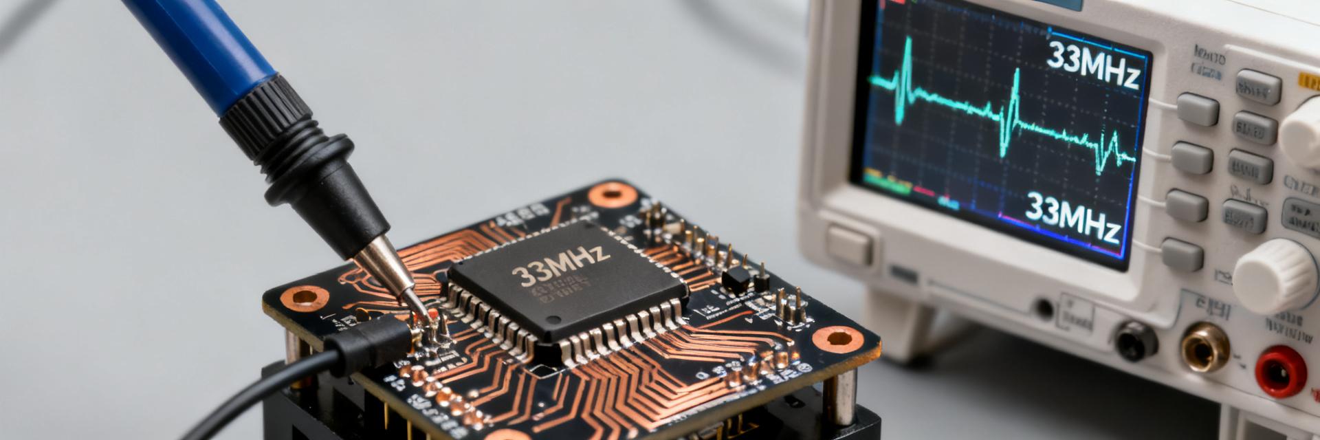
Lab and field measurements for 12 kHz–20 MHz oscillator assemblies show a wide performance spread: typical low‑jitter XOs measure ~40 fs RMS phase jitter while commodity parts can be an order of magnitude worse. This data‑driven report focuses on the 20 MHz XO, aimed at hardware engineers, procurement, and design leads, and is sized for a focused technical read of ~900–1,000 words.
The article breaks down the oscillator specs that matter, compares measured performance envelopes from independent lab runs and datasheet benchmarks, and delivers practical sourcing tips and an RFQ checklist for decisions that balance cost, lead‑time, and reliability.
1 — Background: What a 20 MHz XO Is and Where It’s Used

Core function and common applications
Point: A 20 MHz XO is a packaged crystal oscillator providing a fixed 20.000 MHz clock output. Evidence: Independent lab characterizations and product families show these are commonly used as microcontroller clocks, ADC sampling references, and comms frequency sources. Explanation: Engineers choose fixed‑frequency XOs for low BOM cost and simplicity where a stable, single‑frequency reference reduces downstream PLL complexity.
Key performance terms engineers must know
Point: Engineers must map system needs to frequency tolerance, temp stability, aging, phase noise/jitter, start‑up, and supply sensitivity. Evidence: Test reports and datasheets report units as ppm/ppb for frequency, fs for jitter, and dBc/Hz for phase noise. Explanation: Translating these specs into system budgets (e.g., ADC SNR or link BER) ensures the oscillator specs meet real performance targets.
| Term | Definition | Typical range |
|---|---|---|
| Frequency tolerance | Deviation at room temp | ±5–50 ppm |
| Temp stability | Shift over stated temp | ±10–100 ppm |
| Aging | Drift per year | ±0.5–5 ppm/yr |
| Phase jitter | RMS or integrated fs | 20–400 fs RMS |
2 — Measured Specs & Performance Benchmarks for 20 MHz XOs
Typical spec ranges (benchmarks)
Point: Benchmarks vary by XO class (SPXO/TCXO/OCXO). Evidence: Independent measurements and aggregated datasheet rows show typical ranges: room tolerance ±5–50 ppm, temp stability ±10–100 ppm, aging 0.5–5 ppm/year, phase jitter 20–400 fs RMS. Explanation: Use these envelopes as screening bands — class selection narrows expected jitter and drift.
| Class | Tolerance (typ) | Temp stability | Jitter (RMS) |
|---|---|---|---|
| SPXO | ±20–50 ppm | ±50–100 ppm | 200–400 fs |
| TCXO | ±5–20 ppm | ±10–30 ppm | 40–150 fs |
| OCXO | ±0.1–1 ppm | ±0.1–1 ppm | 10–50 fs |
How to test and validate (recommended measurements)
Point: Testing must cover phase noise, time‑domain jitter, temp sweeps, supply sensitivity, and start‑up. Evidence: Typical lab setups use a phase‑noise analyzer, time‑interval analyzer, temp chamber, and supply‑modulation sources. Explanation: Define acceptance criteria (e.g., integrated jitter <100 fs for ADC budget) and run: phase‑noise plot at offsets (1 kHz–10 MHz), jitter integration bands, chamber ± the required temp range, and modulation at expected supply ripple frequencies against oscillator specs.
3 — Design & Selection Guide: Matching XO Specs to System Requirements
Mapping system-level requirements to oscillator specs
Point: Convert system targets to allowable oscillator parameters via actionable checks. Evidence: Example derivations show SNR‑to‑jitter conversion and tolerance needs for RTC/calendar functions. Explanation: Checklist: derive allowable integrated jitter from ADC SNR, convert timing error budget to ppm for RTC use, and set aging/tolerance from required calibration intervals to decide SPXO vs TCXO vs OCXO.
PCB and layout considerations that affect measured performance
Point: Layout materially affects measured jitter and stability. Evidence: Field tests show adjacent switching regulators or long noisy traces increase spurs and jitter. Explanation: Best practices: keep clock traces short, use solid ground plane, place decoupling within 5 mm of XO Vcc pin, route supply with ferrite + bulk cap, and avoid routing noisy clocks under the oscillator package.
4 — Sourcing Tips & Procurement Strategy for 20 MHz XOs
Where to source: authorized distribution, brokers, and lead-time trade-offs
Point: Source selection balances price, lead time, and traceability. Evidence: Procurement experience shows authorized distributors provide traceability; brokers may offer stock but carry counterfeit risk. Explanation: RFQ checklist: required frequency/tolerance/temp range/aging/jitter, environmental conditions, qualification test requirements, packaging, MOQ, and traceability paperwork. Use sourcing tips to format supplier spec requests and verification steps.
Cost, MOQ, and inventory strategies for production vs. prototyping
Point: Order strategy depends on stage: prototype, pilot, volume. Evidence: Typical MOQ and pricing curves favor larger buys; life‑cycle risk requires buffer stock. Explanation: Recommendations: buy small prototype lots with incoming test screening, pilot buys with additional screening, and volume buys including burn‑in or custom binning; maintain buffer stock sized by forecasted demand and supplier lead times.
5 — Case Examples & Substitutions: When a 20 MHz XO Isn’t Available
Equivalent spec search and safe substitutions
Point: When exact 20 MHz parts are unavailable, safe substitutions require functional and spec parity. Evidence: Designers have used higher‑freq XOs with dividers or matched temp classes successfully. Explanation: Substitution checklist: ensure compatible output type (CMOS/TTL), verify phase‑noise after division, confirm start‑up and pull‑range, and re‑test jitter and spurs in the target system.
Qualification steps for a replacement part
Point: Replacing a qualified part requires a formal requalification plan. Evidence: Effective plans include electrical, environmental, and life screening with statistical sample sizes. Explanation: Validation steps: electrical verification, temp cycling, accelerated aging or MTBF estimation, and update BOM/assembly/test procedures and change notifications to manufacturing.
Summary
- Prioritize jitter, temp stability, and aging when selecting a 20 MHz XO; use benchmark envelopes to pre‑screen candidates and reserve high‑stability classes for tight budgets.
- Validate oscillator specs with phase‑noise plots, integrated jitter, temperature sweeps, and supply‑modulation tests aligned to your system acceptance criteria.
- Use an RFQ checklist and sourcing tips to capture traceability, MOQ, packaging, and qualification requirements up front to reduce procurement risk.
6 — Common Questions
What level of phase jitter should I target for ADC sampling with a 20 MHz XO?
For high‑resolution ADCs aiming for minimal aperture jitter impact, target integrated RMS phase jitter well below 100 fs in the instrument’s critical bandwidth. Convert ADC SNR to allowable jitter, run a phase‑noise integration across the system band, and validate with time‑domain jitter measurements to confirm the oscillator meets that budget.
Can I substitute a different frequency and divide down to emulate a missing 20 MHz XO?
Yes, dividing from a higher frequency can work, but verify resultant phase noise and jitter after the divider — division changes the noise floor and can introduce spurs. Recheck start‑up behavior, divider latency, and output drive compatibility before approving the substitution for production.
What procurement checks reduce counterfeit or lifecycle risk for 20 MHz XOs?
Require traceability from authorized distributors, request certificate of conformity and incoming inspection records, specify lot/sample testing, and include end‑of‑life and lead‑time clauses in RFQs. Maintain alternate approved sources and buffer stock sized by lead time and criticality to reduce lifecycle risk.
How does PCB layout affect the measured jitter of a 20 MHz oscillator?
PCB layout materially affects performance. Best practices require keeping clock traces short, using a solid ground plane, placing decoupling within 5 mm of the XO Vcc pin, routing the supply with a ferrite bead plus bulk capacitor, and avoiding routing noisy digital signals directly under the oscillator package to prevent capacitive coupling and spectral spurs.